Developing the LSI system for the future
Division of Electronics for Informatics
Research Group of Integrated Systems Engineering
Laboratory of Integrated Nanosystems
MC the first year
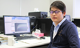
XIE KAN (Nationality:China, Year of enrollment:2013)
Our circumstance is filled with various electronic manufactures such as the mobile telephone, the game console and the digital camera. Those electronic manufactures are developing rapidly in recent decades. The evolution of the performance of those products surprises us. The main reason of evolution of the performance is the high-speed development of the LSI (large-scale integration) technology. However, LSI slows down the speed of development recently because of the limitation of the device’s size.
Our laboratory is applying itself to continue the progress by developing the LSI system for the future. The laboratory consists of three groups, nano device group, image processing group and circuit design group. Members of nano device group are concentrating on the research of nanowire which can be used to create new devices. Circuit design group is responsible for the hardware, such as the imaging sensor. We adopted many new techniques and circuit structure to improve the performance of imaging sensor. At the same time image processing group is responsible for the software.
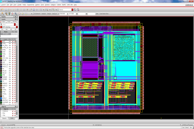
As a member of circuit design group, I’m studying on a high-efficiency Dickson charge pump circuit now. In this study, diode connected MOSFETs is connected to the gate of the charge pump MOSFET driver. The configuration enables boot-strap operation of the driver. So the performance is improved because of the cancellation of threshold-voltage.
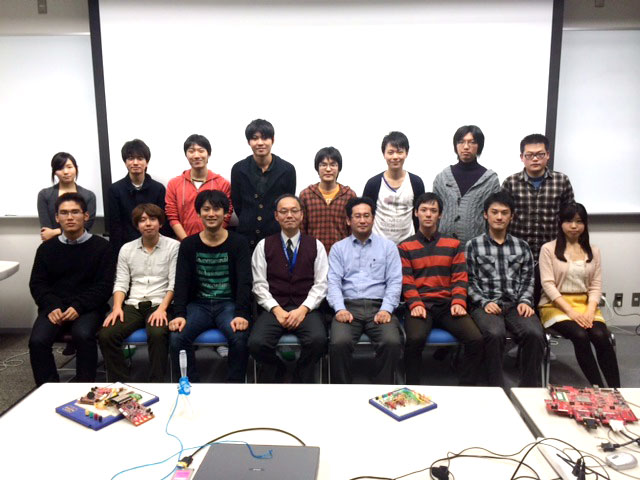
There is a seminar every Friday to provide the opportunity of presentation. Members of our lab will talk about what he is doing or interested in about his research by turn. So it is a good chance to learn about new researches. Also we will have“ nomikai” in some special days. So at that time we can have sufficient communication even if not in the lab.