Leading the world in the development and integration of single-electron transistors and bringing breakthrough by the fusion of information technology and nanotechnology
Fukui Takashi, Doctor of Engineering
Director of Research Center for Integrated Quantum Electronics,
Professor of the Graduate School of Information Science and Technology, Hokkaido University,
Division of Electronics for Informatics's Research Group of Integrated Systems Engineering
LSI integration level that has reached the nano region
The term "nanotechnology" has become widely known, and research and development in the fields of biotechnology and medical care has attracted particular attention in the last few years. I believe that research has also been active in the field of information technology.
Dr. Fukui: It has been half a century since Jack Kilby developed semiconductor integrated circuits in 1958, and these circuits have made dramatic progress in miniaturization and high integration since then. Today, there is even large-scale integration (LSI) with more than 100 million circuit elements packed into a square centimeter, and the element size has already shifted from microns to nanometers. While the realization of central processing units (CPs) with a gate length of 11 nanometers by 2014 is projected by the semiconductor industry road map, a variety of challenges exist in the production of semiconductor devices in the nano region.
One is the problem of the production process. The microfabrication technology in common use today is referred to as the top-down system, in which circuit patterns are written directly on silicon wafers using lithography technology. It is said that the processing size achievable on an industrial basis is limited to approximately 35 nanometers.
Another is the problem of increased power consumption and heat generation caused by high integration. Since several thousand electrons are involved in one transistor of an ordinary semiconductor device, power consumption is naturally large for LSI, which is loaded with nearly 100 million transistors. The amount of heat generation is also enormous as they are integrated in an area of one square centimeter. Development of a new operating principle different from that of conventional integrated circuits is considered necessary to realize further miniaturization, and nanotechnology is expected to play a leading role in it.
The problem of power consumption and heat generation is also related to the global environment and energy resources. What kind of devices can be realized with the new operating principle?
Dr. Fukui: At present, research institutes within and outside Japan are engaged in the development of technology to reduce the current and voltage supplied to LSI, or to reduce the number of electrons involved in the operation of a transistor. The single-electron transistor, which uses only one electron for on-off control, is attracting particular attention. Power consumption is expected to decrease to 1/10,000th that of conventional devices with the realization of this technology.

An ultimate digital device that uses only one electron for on-off control
Dr. Fukui: A single-electron transistor produces an on or off status by creating conductor islands (dots) of approximately 10 nanometers in diameter on a very small semiconductor base and charging/discharging one electron to and from each dot. Since it uses the Coulomb blockade phenomenon (in which the potential of a dot is increased by charging an electron and stopping other electrons from entering), it is also known as an ultimate energy-saving transistor (Ex. 1).
While the theory of the single-electron transistor itself had already been presented at the end of the 1980s, it was considered unfeasible with the technology of the period, since processing to reduce the dot size to approximately 10 nanometers was necessary for operation at room temperature. However, the advance of microfabrication technology in the 1990s enabled the production of a variety of nanostructures, and attempts to realize single-electron transistors began in many countries.
Only one single-electron transistor was created at first as a product of coincidence, and was not usable as a circuit element. Transistors for use as integrated circuits must be produced not only to demonstrate the physical theory, but also to seek a way for practical application. Our aim was to develop single-electron transistors that can be integrated to function as a logic circuit. While many researchers worked on single-electron transistors made of silicon (since most common semiconductor devices are made of silicon), our laboratory uses compound semiconductors consisting of chemical compounds with gallium, indium and other metals.
You have been engaged in research on compound semiconductors for over 30 years since the development of a semiconductor laser at the NTT Laboratory. What are the advantages of a single-electron transistor using compound semiconductors?
Dr. Fukui: To integrate transistors, it is necessary to precisely design their positional relationship. However, microfabrication on a scale of several tens of nanometers is not possible with the conventional top-down system. What can be useful here is a bottom-up system to form a nanostructure through self-organized growth of atomic and molecular crystals contrary to the top-down system.
Compound semiconductors are suited for formation of a bottom-up-type microscopic circuit network, and their fabrication technology is mature. We have realized a nanostructure with a dot diameter and conductor width of several tens of nanometers. It has a well-designed layout using a technology called organometallic vapor phase selective epitaxy (Ex. 2), which combines the top-down and bottom-up systems. We succeeded in confirming the operation of an AND/NANO logic circuit by integrating four single-electron transistors in an experiment in 2003. In 2005, we were also successful in producing an AND/XOR one-bit adder that works with three transistors.
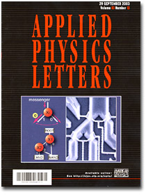
The results of these experiments were presented in Applied Physics Letters, the American Physical Society's journal of academic papers, with the cover featuring an electron micrograph of a logic circuit formed by integrating single-electron transistors (Photo 1). I think this is a world-class research achievement that realizes a truly ultimate digital device.
As a key technology of the 21st century
I think the realization of a single-electron transistor will have a strong impact on current information technology. What are your thoughts on the possibility of putting it into practical use?
Dr. Fukui: More than 100 million transistors are integrated in the CPUs of currently used PCs, and it would not be easy to replace them with single-electron transistors immediately. Although silicon single-electron transistors suitable for integration and those made of carbon nanotubes have also been developed in recent years, they cannot be put into practical use yet and it is necessary to wait for future advances in research and development.
The significance of these research efforts, however, lies in the actual creation of something that was previously only a prediction and a theoretical demonstration. The single-electron transistor plays the role of a test device in investigating what kind of phenomena will actually occur when the number of electrons related to transistor operation is reduced to the minimum. The Ministry of Education, Culture, Sports, Science and Technology also positions the research and development of nano devices, materials and systems in the field of information processing/communication as a priority target, allocating a large research budget to this field. It is highly valued as a groundbreaking research project focused on the future.
Hokkaido University has already established an advanced research system in the field of nanotechnology. Research has been conducted at a variety of facilities, including the Research Center for Integrated Quantum Electronics, the Nanotechnology Research Center and the Catalysis Research Center. Against this background, what kind of development will there be at the Graduate School of Information Science and Technology concerning nanotechnology?
Dr. Fukui: A. Nanotechnology can be applied to a wide variety of fields, including information technology, biotechnology, medical care, the environment and energy. While the Graduate School of Information Science and Technology focuses on nanotechnology in the sense of becoming a leader of information technology hardware, there is also a possibility of creating completely new theories or technologies through organic cooperation among researchers in various fields by taking advantage of the strengths of the university. There is no doubt that nanotechnology will become a key technology of the 21st century, and we researchers believe that it is our task to achieve breakthroughs to dramatically improve the issues faced by modern society.
Explanation
Explanation 1: Mechanism of a single-electron transistor
Conductor islands (dots) of approximately 10 nanometers in diameter are placed between the source and drain electrodes across a tunnel barrier. When an electron flows into a dot, the potential of the dot increases and the entry of other electrons is hindered by the Coulomb blockade phenomenon. Voltage applied to the gate electrodes controls the electrons in the dots and determines the on/off status of the current. In an AND/NAND logic circuit using four single-electron transistors or an AND/XOR one-bit adder using three, the circuit architecture is changed from the conventional logic gate to a binary decision graph suitable for single-electrons.
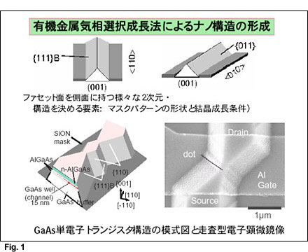
Explanation 2: Organometallic vapor phase selective epitaxy
This is a type of thin-film crystal growth method for compound semiconductors, in which gaseous organometallic and hydrogen compounds are used as sources. When these sources are sent onto a heated substrate crystal using hydrogen as a carrier gas, the thermally decomposed source gas grows in a thin-film form. In this study, a circuit diagram of 150 nanometers in width was drawn using electron lithography and etching (used for conventional semiconductor processing) and a GaAs (gallium arsenide) crystal was grown on it. The crystal can be grown to form a mountain shape by controlling the direction of its development through adjustment of temperature and other conditions, and the ridge part of the mountain has a width as small as several tens of nanometers. Evaporating a metal to serve as a conductor on this structure produces a single-electron transistor (Fig. 1).