The following experimental facilities are used in our laboratory.
Crystal growth and thin film deposition
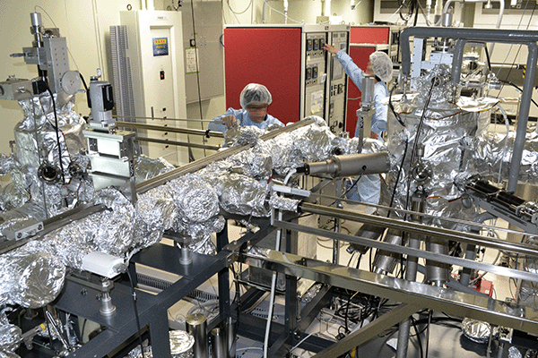
The III-V compound semiconductor molecular beam epitaxy system and the ultra-high vacuum electron beam deposition system are connected by an ultra-high vacuum transport tunnel to make it possible to perform epitaxial growth using an all-in-vacuum process. High quality crystals with atomically controlled film thickness such as GaAs and InGaAs quantum dots, quantum wells and superlattices for optical device fabrication are grown. Doping and growth of dilute nitride semiconductors (GaNAs) using nitrogen plasma are also possible. After fabricating device structures using semiconductors, it is possible to stack electrode structures and other components by electron beam evaporation without breaking the ultra-high vacuum environment.
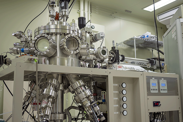
UHV sputtering equipment for thin film fabrication of metallic ferromagnets and oxides. It has a load lock chamber to maintain ultra-high vacuum conditions in the sputtering chamber. The long throw sputtering (long distance sputtering), which increases the distance between the sample substrate and the sputter source, reduces plasma damage and enables the formation of ultra-thin films at the several-atomic layer level.
Heat treatment
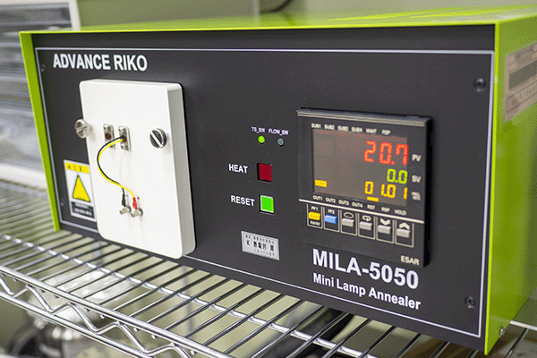
Maximum heating temperature: 1200°C, Temperature increase rate: 50°C /s, Sample dimensions: 50 x 50 mm t5 mm, Heating atmosphere: Vacuum, Nitrogen
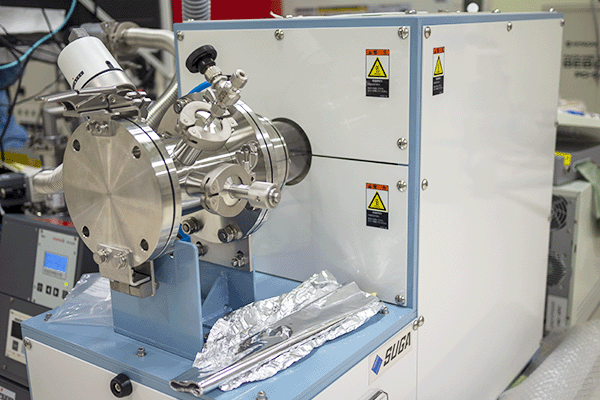
Large heating chamber volume enables heat treatment of a large number of specimens or components for ultra-high vacuum at a time.
Maximum temperature: 1000°C, Heating atmosphere: Vacuum
Self-made Ultra-fast Time-resolved Photoluminescence Spectroscopy System (for near-infrared)
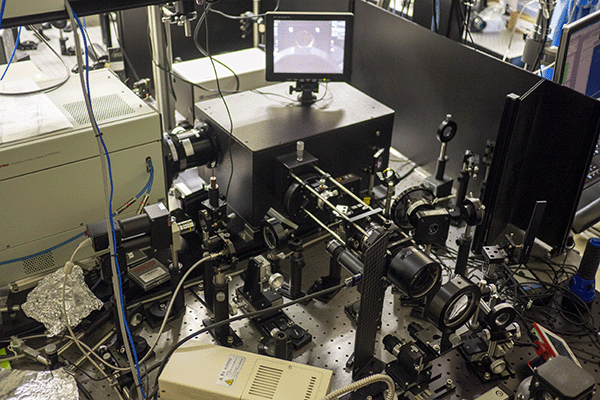
This system enables time-resolved measurement of photoluminescence spectra, mainly in the near-infrared region, in the ultrafast time domain on the order of 1 picosecond. Time variation of polarization characteristics can also be detected.
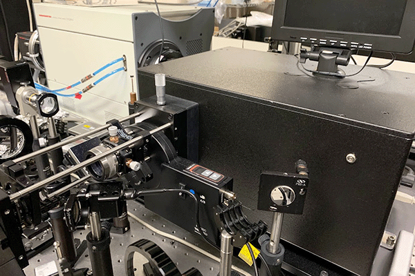
Time-resolved spectroscopy of photoluminescence in the visible to near-infrared region.
Wavelength range: 300 -1300 nm, Time range: 0.3 - 2 ns, Time resolution: about 2 - 20 ps
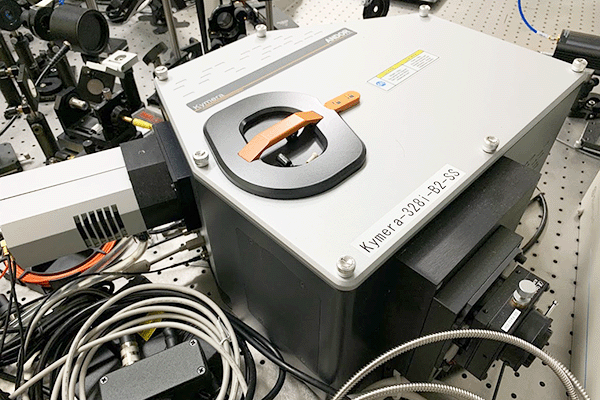
A set of monochromator and detector for near-infrared light. This instrument and streak camera can be switched by a mirror.
Wavelength range: 900 - 1700 nm
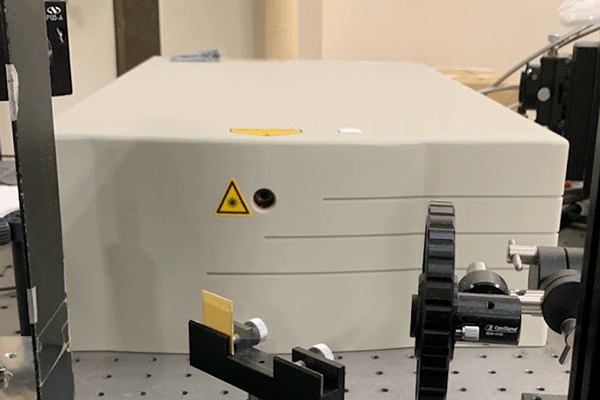
Wavelength tunable Ti:sapphire femtosecond pulsed laser controlled by computer. It is used as a excitation light source for time-resolved photoluminescence spectroscopy. Combined with a harmonic generator, it can also provide 2nd and 3rd harmonic wavelength converted output.
Wavelength: 690 - 1040 nm, Repetition rate: 80 MHz, Pulse duration: < 100 fs
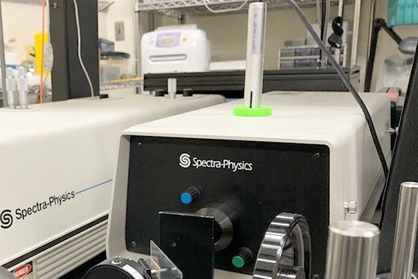
Wavelength-tunable Ti:sapphire CW laser. It is used as an excitation light source for photoluminescence measurement.
Wavelength: 700 - 1000 nm
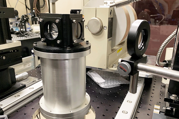
A custom-built closed-cycle cryostat that can also heat samples. Temperature can be set continuously from cryogenic to 200°C. Equipped with current induction terminals (4-wire).
Temperature: 4 - 473K
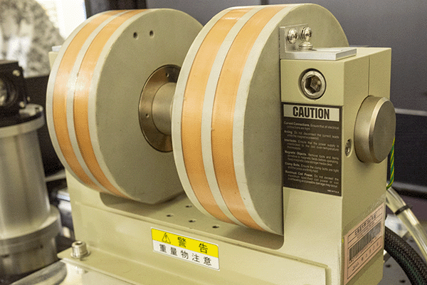
A magnetic field can be applied to the sample during photoluminescence spectroscopy measurements. The guide rail allows easy measurement without readjustment of the optical axis by swapping places with the cryostat. The pole piece gap, which determines the maximum magnetic field, can be changed.
Magnetic field: up to 2.1 T (at 10 mm poll piece gap), Forked arrangement for photoluminescence measurements on thin film samples
Self-made Ultra-Fast Tme-resolved Photoluminescence Spectroscopy System (for visible)

This system enables time-resolved measurement of photoluminescence spectra at ultrahigh speeds of up to picoseconds. A switchable mirror inside the spectrometer allows selection between a streak camera for time-resolved measurements and a regular CCD detector for measurements.
Wavelength range: 200 - 900 nm, Time range: 0.3 ps - 1 ms, Time resolution: min. about 2 ps
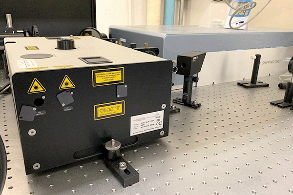
Wavelength tunable femtosecond pulsed laser controlled by computer. It is used as an excitation source for photoluminescence spectroscopy. Pulse selector and harmonic generator are also available. It has extremely wide wavelength tunability and group velocity dispersion compensation mechanism.
Wavelength: 340 - 650, 680 - 1300 nm, Repetition rate: 1 kHz - 80 MHz, Pulse width: < 120 fs
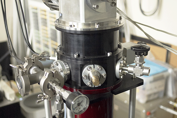
This is a closed-cycle cryostat capable of cooling samples up to 4K. Helium gas can be introduced into the sample cell, enabling cooling in a gas atmosphere. Not only solid samples but also powder samples can be cooled by sealing them in a glass tube.
Temperature: 4.2 – 300K
Self-built Microspectroscopy System in Magnetic Field
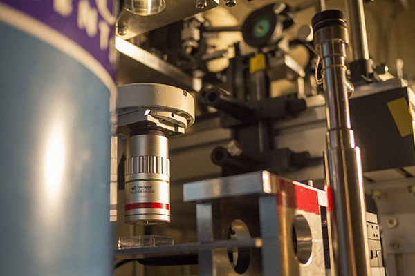
The objective lens of the microscope is used to focus the spot diameter of the excitation laser to selectively excite a small area of the sample. The position of the excitation spot can be observed using coaxial epi-illumination and an observation camera.
If a magnetic field is not required, a small cryostat can be used for easy measurement at cryogenic temperatures. For device samples such as LEDs, current injection emission (EL) spectroscopy can be performed from specific micro-regions in the device structure.
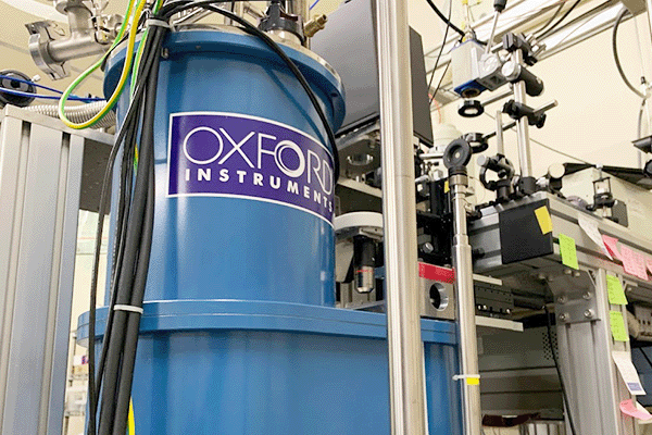
An external magnetic field can be applied to the sample. A liquid helium continuous flow cryostat can be used to cool the sample.
Magnetic field: 0 - ±5 T (Faraday arrangement)
Temperature: 4.2 – 300K
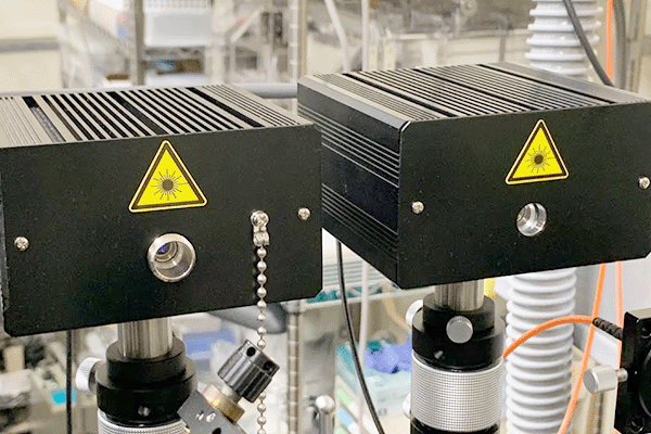
A semiconductor laser that can switch between CW and pulsed operation.
Laser head wavelengths: 405, 780, 850 nm Minimum pulse width: 40 - 80 ps
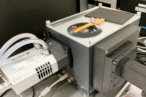
A set of monochromator and InGaAs detector for near-infrared light.
Wavelength range: 900 - 1700 nm
Measurement of Electrical Characteristics
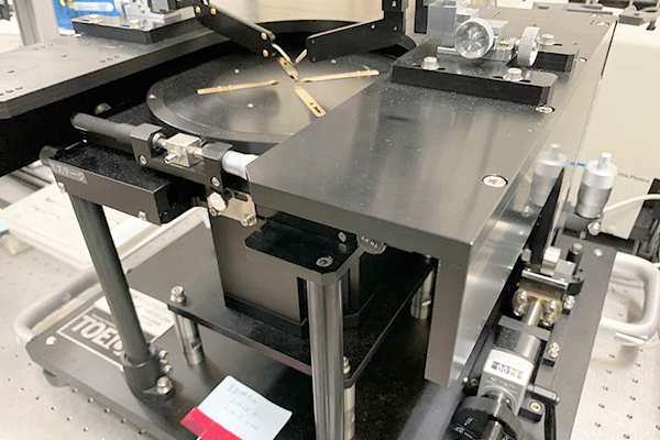
A manual prober that can apply a magnetic field perpendicular to the film surface of a thin film sample and perform various electrical measurements.
Magnetic field: 0 – ±0.4 T
