
Quantum Dots Connecting Electrons and Light to Open Up the Future of "Photoelectric Information Conversion"
Today's advanced information society is supported by computing (electronic information processing) and the Internet (optical communications). Therefore, "photoelectric information conversion," which exchanges information between the two, is very important. For the society of the future, it is expected to realize technologies that convey realistic and three-dimensional image information with authentic texture as we wish. Furthermore, the complex and extremely narrow electrical signal wiring of 3D, ultra-highly integrated electronic circuits that support advanced information processing such as AI and Big Data causes significant signal speed delays. In addition, heat generation, or loss of electric energy due to electrical resistance, has become a major social problem. Therefore, research is also being conducted on opto-electronic fusion integration (optical wiring) technology, which replaces such electrical signal wiring with optical signals.
Therefore, there is a strong need to pioneer innovative "photoelectric information conversion" technology with high performance and extremely low power energy consumption. In this laboratory, we are researching nano electronic materials and optical devices essential for such future-oriented "photoelectric information conversion," as well as fundamental technologies for completely new photoelectric fusion information systems.
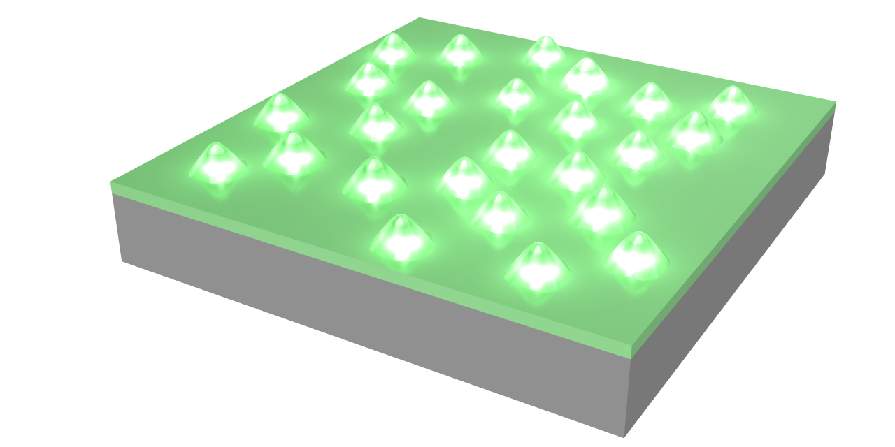
The electronic materials we are focusing on are semiconductor quantum dots. Quantum dots are semiconductor crystals of only a few dozen nanometers in size (each atom is 0.1 nanometer in size). If we can fabricate clean crystals of these quantum dots in a highly uniform and dense manner, we can realize high-performance light-emitting diodes (LEDs) and laser devices that consume much less electric energy.
We will pioneer future "photoelectric information conversion" systems by exploring various new nanoelectronic materials such as these quantum dots and researching and developing photoelectric conversion devices with unprecedented high performance and low power consumption.
Photoelectric Spin Information Conversion Using Quantum Dots
By using semiconductor quantum dots, it is possible to realize a new photoelectric information conversion system that mutually converts the spin information of electrons and the spin information of light, i.e., circular polarization properties. Currently, spintronics (electronics technology using spin states) using metallic ferromagnetic materials such as iron (Fe), which can generate electron spin information at room temperature, is being actively researched. Spin is a property of a magnet, so to speak, that has information on the polarization of its direction (called spin polarization) and is kept stable in ferromagnetic materials. This means that energy-saving electronic circuits, such as memory, can be realized that do not require power consumption.
On the other hand, since optical devices cannot be fabricated from metallic ferromagnetic materials, we are developing spin-polarized light-emitting diodes (spin LEDs) that can directly convert electron spin information into circularly polarized light for optical transmission.
Related Papers
-
Influence of bias voltage on the performance of polarization sensitive near-infrared photodiode based on dilute nitride GaNAs
D. Mineyama, T. Yano, K. Etou, K. Nakama, H. Hashimoto, K. Minehisa, J. Takayama, A. Subagyo, K. Sueoka, F. Ishikawa, A. Murayama, and S. Hiura
Applied Physics Letters 126, 223507:1-7 (2025). [doi] -
Efficient Room-Temperature Operation of a Quantum Dot Spin-Polarized Light-Emitting Diode under High-Bias Conditions
K. Etou, S. Hiura, S. Park, J. Takayama, A. Subagyo, K. Sueoka, A. Murayama
Physical Review Applied 19 024055:1-9 (2023). [doi] [PRESS RELEASE] -
Room-temperature spin transport properties in In0.5Ga0.5As quantum dot spin-polarized light-emitting diode
K. Etou, S. Hiura, S. Park, K. Sakamoto, J. Takayama, A. Subagyo, K. Sueoka, and A. Murayama
Physical Review Applied 16, 014034 (2021). [doi]
[PRESS RELEASE]
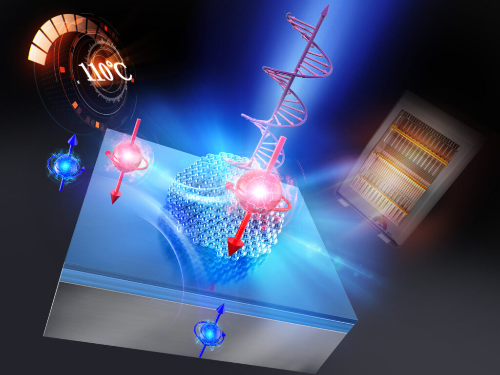
Novel Quantum Dot Amplifies Electron Spin Polarization
We have recently realized, in collaboration with overseas groups, new quantum dot materials that can efficiently amplify and restore electron spin information (spin polarization) in semiconductors, which is easily lost at room temperature, over a temperature range from room temperature to even 110 degrees Celsius. We have also proposed a spin-LED that utilizes such spin-amplified quantum dots.
Related Papers
-
Effect of dilute nitride GaNAs quantum well thickness on spin amplification dynamics of tunnel coupled InAs quantum dots
S. Sato, S. Hiura, J. Takayama, and A. Murayama
Applied Physics Letters 123, 232405:1-7 (2023). [doi] -
Room-temperature spin transport properties in In0.5Ga0.5As quantum dot spin-polarized light-emitting diode
K. Etou, S. Hiura, S. Park, K. Sakamoto, J. Takayama, A. Subagyo, K. Sueoka, and A. Murayama
Physical Review Applied 16, 014034 (2021). [doi]
[PRESS RELEASE] -
Room-temperature electron spin polarization exceeding 90% in an opto-spintronic semiconductor nanostructure via remote spin filtering
Y. Q. Huang, V. Polojärvi, S. Hiura, P. Höjer, A. Aho, R. Isoaho, T. Hakkarainen, M. Guina, S. Sato, J. Takayama, A. Murayama, I. A. Buyanova, and W. M. Chen
Nature Photonics 15, 475-482 (2021). [doi]
[PRESS RELEASE]
Optical Spin Modulated Electric Field-effect Devices
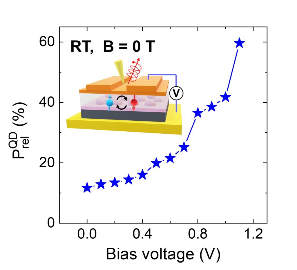
In conventional nonmagnetic semiconductors, controlling electron spin requires the application of a strong external magnetic field of several tesla (T). We are now working on ultrafast control of electron spin polarization by electric field manipulation, a fundamental technology in electronics, without the need for such a magnetic field. This research will lead to the development of integrated polarization modulators that can operate in the gigahertz (GHz) frequency range.
Related Papers
-
Electric-field driven source of photocarriers for tunable electron spin polarization in InGaAs quantum dots
H. Kise, S. Hiura, S. Park, J. Takayama, K. Sueoka, A. Murayama
Applied Physics Letters 122, 232405:1-7 (2023). [doi]
(selected as an Editor’s Pick) -
Efficient Room-Temperature Voltage Control of Picosecond Optical Spin Orientation Using a III-V Semiconductor Nanostructure
S. Park, S. Hiura, J. Takayama, K. Sueoka, and A. Murayama
Advanced Electronic Materials 8, 2200588 (2022). [doi] -
Electric field control of spin polarity in spin injection into InGaAs quantum dots from a tunnel-coupled quantum well
H. Chen, S. Hiura, J. Takayama, S. Park, K. Sueoka, and A. Murayama
Applied Physics Letters 114, 133101 (2019). [doi]
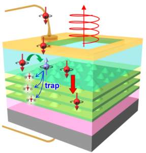
Novel Hybrid Nanostructures of Zero-dimensional Quantum Dots and Two-dimensional Electron Systems
The quantum mechanical coupling of nanostructures with different dimensionality of quantum confinement for electrons through tunneling effect leads to innovative functions that can never be achieved by these nanostructures on their own. We have proposed a unique hybrid nanostructure consisting of a zero-dimensional quantum dot and a two-dimensional electron system, a quantum well, to study novel electron spin properties and optical functionality.

Related Papers
-
Effect of dilute nitride GaNAs quantum well thickness on spin amplification dynamics of tunnel coupled InAs quantum dots
S. Sato, S. Hiura, J. Takayama, and A. Murayama
Applied Physics Letters 123, 232405:1-7 (2023). [doi] -
Efficient Room-Temperature Voltage Control of Picosecond Optical Spin Orientation Using a III-V Semiconductor Nanostructure
S. Park, S. Hiura, J. Takayama, K. Sueoka, and A. Murayama
Advanced Electronic Materials 8, 2200588 (2022). [doi] -
Room-temperature electron spin polarization exceeding 90% in an opto-spintronic semiconductor nanostructure via remote spin filtering
Y. Q. Huang, V. Polojärvi, S. Hiura, P. Höjer, A. Aho, R. Isoaho, T. Hakkarainen, M. Guina, S. Sato, J. Takayama, A. Murayama, I. A. Buyanova, and W. M. Chen
Nature Photonics 15, 475-482 (2021). [doi]
[PRESS RELEASE]
"Top-Down" Quantum Dots Fabricated Using Biotechnology
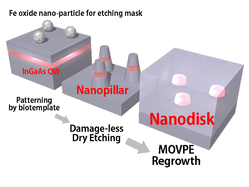
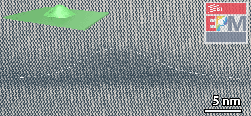
Semiconductor quantum dots have a strong confinement effect on electrons, so their optical performance, including laser oscillation characteristics, is maintained even at room temperature and high temperatures, making them a promising material for future optical devices. They are also beginning to be put into practical use. However, since the size of quantum dots is very small, a high-density dot array structure is essential to achieve high practical performance. In collaboration with other universities, we are applying biotechnological techniques to design the size and shape of quantum dots in a top-down approach and fabricate quantum dot optically active layers with extreme high density.
Related Papers
-
Photoluminescence of InGaAs/GaAs Quantum Nanodisk in Pillar Fabricated by Biotemplate, Dry Etching, and MOVPE Regrowth
Akio Higo, Takayuki Kiba, Junichi Takayama, Chang Yong Lee, Cedric Thomas, Takuya Ozaki, Hassanet Sodabanlu, Masakazu Sugiyama, Yoshiaki Nakano, Ichiro Yamashita, Akihiro Murayama, Seiji Samukawa
ACS Applied Electronic Materials 1, 1945 (2019). [doi] -
Optical Study of Sub-10 nm In0.3Ga0.7N Quantum Nanodisks in GaN Nanopillars
Akio Higo, Takayuki Kiba, Shula Chen, Yafeng Chen, Tomoyuki Tanikawa, Cedric Thomas, Chang Yong Lee, Yi-Chun La, Takuya Ozaki, Junichi Takayama, Ichiro Yamashita, Akihiro Murayama, and Seiji Samukawa
ACS Photonics 4, 1851 (2017) [doi]
Time-resolved Photoluminescence Measurements and Excited Electronic States of Novel Chemical Molecular Materials
In collaboration with the Graduate School of Science, Hokkaido University, we are conducting time-resolved photoluminescence measurements of newly synthesized complex compounds to elucidate the electronic states induced by photoexcitation. Through such research, we will develop new photo-functional molecular materials that exhibit high-brightness and luminescence properties that vary depending on the chemical environment and thermal history.
Related Papers
-
Enhancement of Emission Efficiency and Color Tuning by Mixing Platinum(II) and Palladium(II) Complexes in a One-dimensional Chain
K. Segawa, M. Yoshida, H. Kise, J. Takayama, S. Hiura, A. Murayama, S. Okabayashi, M. Tsuboi, T. Tachikawa, K. Onda, and M. Kato
Angewandte Chemie International Edition e202513282 (2025). [doi] -
Vapor‐Induced Assembly of a Platinum(II) Complex Loaded on Layered Double Hydroxide Nanoparticles
T. Morimoto, M. Yoshida, A. Sato-Tomita, S. Nozawa, J. Takayama, S. Hiura, A. Murayama, A. Kobayashi, and M. Kato
Chemistry – A European Journal 29, e202301993:1-8 (2023). [doi] -
Thermo- and Mechano-triggered Luminescence ON/OFF Switching by Supercooled Liquid/Crystal Transition of Platinum(II) Complex Thin Films
M. Yoshida, V. Sääsk, D. Saito, N. Yoshimura, J. Takayama, S. Hiura, A. Murayama, K. Põhako-Esko, A. Kobayashi, and M. Kato
Advanced Optical Materials 2102614:1-9 (2022). [doi]