The cutting edge of next-generation optical network technology led by nanophotonics
Masanori Koshiba, Doctor of Engineering,
Professor of the Graduate School of Information Science and Technology, Hokkaido University,
Division of Media and Network Technologies's Research Group of Information Communication Systems
Ubiquitous society - what's next?
Broadband has recently spread to general households, and the term "photonics" is becoming established. What kind of research is currently conducted at the cutting edge of optical network technology?

Dr. Koshiba: Since Japan has conventionally played a leading role in the research and development of optical communications, its industry, educational institutions and administration all have world-class technical capabilities. Hokkaido University has also made many achievements in developing advanced technologies in the field of photonics. This foundation is currently being built on in the field of information through the Graduate School of Information Science and Technology, and research toward the realization of a next-generation optical network is being promoted from a comprehensive point of view, including communications, electronics and information technology.
Optical networks are an essential technology in ubiquitous society, and FTTH service to spread optical fibers to general households is also expanding dramatically. There is, however, a major problem in that the further spread of optical networks in the future may cause a huge increase in the amount of information distributed on the net and possibly even exceed Moore's Law. While the optical fibers currently in use are capable of terabyte transmission (i.e. transmission of 1 trillion optical pulses per second) by wavelength division multiplexing (Ex. 1), the capacity of the fiber is used to its limit. It is also expected that the electric signals used to process switching, routing and other network transfer functions will not be able to keep up with the speed of optical signals in the future.
Against this background, a new optical technology using photonic crystals (Ex. 2) is attracting attention as a key method of speeding up next-generation optical networks. While photonic crystals themselves are present in the natural world, nano-sized photonic crystals can now be produced artificially with the dramatic advances in nanophotonics technology supported by the recent evolution of nanotechnology. This is expected to lead to the realization of various optical devices, including entirely new optical fibers with properties that cannot be realized by conventional optical fibers and microminiature optical circuits.
A nano-sized periodic structure to control the refractive index of light
What is a photonic crystal?
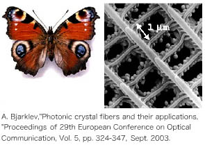
Dr. Koshiba: A number of examples of photonic crystals are found in daily life. One instance is the beautiful colors of butterfly wings (Photo 1) and opals. These are the result of a phenomenon known as Bragg reflection, which involves the strong diffraction or reflection of light of a certain wavelength in a specific direction. Such substances with periodic structures that reflect and transmit only light of specific wavelengths are called photonic crystals. While those with one-dimensional periodic structures have already been put to practical use in applications such as dielectric multilayer filters, we are now studying photonic crystals with two- or three-dimensional periodic structures. Using these will make it possible to create new optical fibers and circuits. Particular advances are being made in the research and development of photonic crystal fibers as a technology close to practical application.
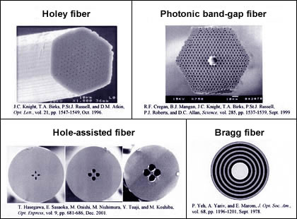
A conventional optical fiber is a glass filament of approximately 125 micrometers (1 micrometer is 1/1,000 millimeter) in diameter. It has a central core through which light can pass, and a cladding layer with a different refractive index surrounds it. While a photonic crystal fiber is basically the same, multiple holes are positioned systematically in the clad region. Since these holes have periodic structures based on the wavelengths of light, the refractive index of light can be controlled by appropriately adjusting the size and arrangement of the holes. There are two types of photonic crystal fibers - the total reflection type with a glass core and a band gap type with a hollow core (Photo 2), which feature many properties not found in conventional fibers.
Photonic crystal fibers with complete control over the loss and dispersion of light
What specific properties does it have?
Dr. Koshiba: The most remarkable property is that it can minimize the loss of light and freely control the dispersion that hinders high-speed transmission. It can let through light of wavelengths that cannot be transmitted with an ordinary optical fiber, and almost entirely eliminates loss caused by bending. The bandgap type has a hollow core, and the refractive index of light becomes smaller in the air it contains. Although light should not normally be trapped in the core section because of its property of becoming trapped in places with a large refractive index, it stays inside on the principle of Bragg reflection since the surrounding cladding layer serves as a photonic crystal. Also, since light loss in above-ground environments is at its smallest in air, light is transmitted through the core with almost no loss. In other words, photonic bandgap fiber may represent the ultimate low-loss transmission line that mankind can achieve.

What are the advantages of photonic crystal fiber over conventional optical fiber?
Dr. Koshiba: First, it is resistant to bending because of the holes in the clad layer. The bending loss of conventional optical fiber increases dramatically when the bending radius becomes 20 millimeters or smaller. This radius is therefore limited to approximately 30 millimeters at the time of wiring. Conversely, photonic crystal fiber has minimal bending loss and can be bent almost at a right angle (Fig. 1 is a graph showing the extremely low bending loss), thus making high-density wiring or indoor extension / wiring easy.
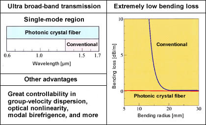
Second, the wavelength range that can be transmitted on a single mode is much broader than that of the conventional type. While conventional fibers use invisible light in a near-infrared region with wavelengths of 1.3 to 1.7 micrometers, photonic crystal fibers can use light of up to 0.4 micrometers, which is in the range of visible light. The availability of a broader band is exactly what leads to the efficient use of frequency resources. These fibers also have other advantages (such as the ability to flexibly control nonlinearity and realization of a high polarization-maintaining property), and steady and precise processing is also possible as they are made of high-quality glass.
Such properties also make photonic crystal optical circuits greatly advantageous. In the optical fiber systems currently in use, light of different wavelengths is multiplexed and transmitted to one optical fiber by wavelength division multiplexing as mentioned at the beginning. When the number of multiplexed wavelengths becomes too large, however, the size of the optical multiplexer/demultiplexer that multiplexes/demultiplexes light at the entrance and exit of transmission may become too big. Photonic crystal optical circuits are thought to solve this problem. Since light can be transmitted without loss using photonic crystals even if its path is bent at a right angle, it is possible to form an optical circuit similar in size to a conventional integrated circuit. It is considered possible to use this as a platform for future ultra-high integrated optical circuits.
In the tenth year since the creation of photonic crystal fibers, now is the time to expand its application to technologies that benefit society.
Photonic crystal technology is expected to play a leading role in the next generation of optical networks. What kind of development is expected in terms of commercialization and practical application for the technology?

Dr. Koshiba: It has been almost 15 years since the emergence of the concept of photonic crystals, and 10 years since the creation of the first photonic crystal fiber. The development of optical communications technology is a national policy, and basic research in the field of nanophotonics has been led by industry, educational institutions and the administration. It is now time to produce products that can be used in the real world. NTT is already putting holey fibers based on total internal reflection into practical application and is preparing to commence an access-system service. Our laboratory is also shifting to a research phase for practical application of photonic crystal fibers. Besides the fibers, we are also engaged in research and development of microminiature photonic crystal optical circuits that can withstand wavelength division multiplexing. The possibility of application for photonic crystal fibers is also expanding outside the field of communications. We hope to establish it as a technology to contribute to society while keeping the expansion of its fields of application in mind.
Explanation
Explanation 1: Wavelength division multiplexing
Wavelength Division Multiplexing (WDM) is a type of communication technology using optical fiber. By transmitting multiple optical signals (i.e. light with various wavelengths) simultaneously, it is possible to put more data on a single fiber. Optical signals processed by a multiplexer are transmitted on an optical fiber and are re-separated into the original multiple optical signals by a demultiplexer on the receiving side. While arrayed waveguide grating (AWG) is mainly used for multiplexing/demultiplexing light at present, the device size becomes larger with an increased number of multiplexed wavelengths. Since a photonic crystal optical circuit can transmit light along a path without loss, even if bent at a right angle, it is attracting attention as a new technology that can withstand increased wavelengths.
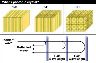
Explanation 2: Photonic crystal
A photonic crystal has a periodic structure based on the wavelength level of light. There are one-, two- and three-dimensional structures. Similar to the occurrence of a band gap in the energy levels of electrons due to the periodic potential of the nucleus, a photonic band gap of electromagnetic waves occurs in a photonic crystal, and light can be confined, bent sharply or branched easily by creating point, line and other arbitrary defects. With the advance of nanotechnology, it has become possible to create nanometer-size periodic structures artificially. Photonic crystal fibers with several dozen to more than one hundred holes in a section approximately 125 millimeters in diameter have also been realized.