Laboratory outline
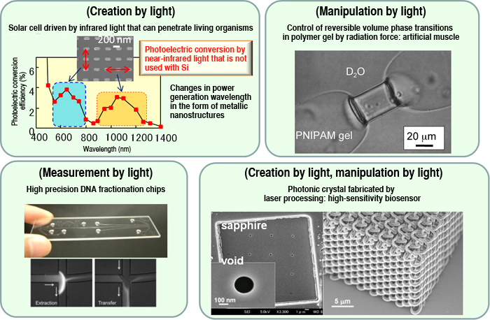
Light is useful for the measurement and treatment of living organisms (laser scalpel, eye surgery, etc.). In our group, studies on light-matter coupling processes and photochemistry related to light energy conversion are conducted, in search of bioengineering. In the research field of photochemistry, the new concept that molecules absorb a photon efficiently is now attracting attention as the “effective utilization of photons.” We have launched a new research field referred to as plasmonic chemistry which focuses on optical antennas (metallic nanostructures) that can enhance electromagnetic field by localized surface plasmon resonance as photochemical reaction fields that enhance light-matter coupling and allow for the effective utilization of photons. In this research, we have clarified the effects of light harvesting by metallic nanostructures and localizing it at nanometer-sized minute space as follows: Non-linear photochemical reactions become possible by a weak incoherent light source such as sunlight; and low-energy visible light and near-infrared light can be used for light-energy conversion systems such as solar cells and artificial photosynthesis.
Specific research themes include plasmonic chemistry-related subjects (near-infrared solar cells, artificial photosynthesis, plasmonic nanolithography, terahertz sensor, etc.), in which many laboratory members are involved, femtosecond laser processing, the development of hotonic devices, molecular manipulation by laser trapping, and the development of a microanalytical system for gene diagnosis (DNA fractionation chip).
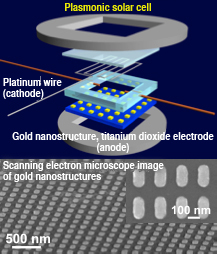
- Development of a solar cell driven by infrared light that can penetrate living organisms (the cell is implanted into the living body, and can be charged by infrared light irradiation from outside the body)
- Molecular manipulation by laser trapping
- Development of a microanalytical system using microfabrication technology
- Development of microphotonic devices that can be applied to biomolecular microanalysis using femtosecond laser processing and photonic crystals
Introduction of research content
Near-infrared solar cell/artificial photosynthesis
It is known that near-infrared light at wavelengths of 800 to 1,100 nm can easily penetrate living organisms. We aim to develop a solar cell equipped with a nanometer-sized optical antenna (metallic nanostructure) that can harvest near-infrared light, and then to develop an implantable solar cell to which energy can be supplied from outside the body. Using this system, we plan to advance research with a view to applying it to artificial photosynthesis systems such as the complete water splitting (evolution of both hydrogen and oxygen) by infrared light irradiation and the fixation of carbon dioxide.
Femtosecond laser processing
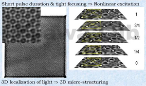
Non-linear optical phenomena such as multiphoton absorption and quantum phenomena including tunnel ionization can easily be observed under high-photon density conditions created by a focused femtosecond laser. Using this, we studied on three-dimensional fabrication with super resolution, for which only the inside of transparent material is produced without damaging the surface with resolution under the diffraction limit of light to fabricate 3D memories, photonic crystals and microchannel chips. We also study semiconductor processing, including silicon, metal such as stainless steel, and ceramics such as single crystal sapphire.
Photonic crystal
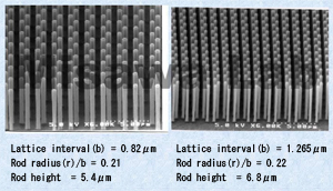
By semiconductor processing technology and aluminum anodic oxidation, we fabricate submicron periodic structures called photonic crystals (2D) that can trap light, and studied their optical properties. We also fabricate 3D photonic crystals that can trap more light by self-organized periodic polymer microparticles and femtosecond laser processing, and studied their optical properties. We use these various photonic crystals to build new optical waveguide structures, microscopic laser resonators and photochemical reaction fields.
Examples of research equipment
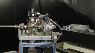
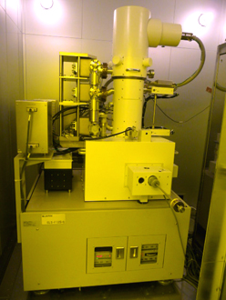
Knowledge and technologies that will be useful in the future
Basic technologies for bio-related research and development
- DNA manipulation technology
- Optical microscope, confocal/multiphoton microscope technology
Technologies and knowledge necessary for nanotechnology-related research and development
- Semiconductor microfabrication technology
- Electron microscope technology
- Atomic force microscope technology
- Time-resolved spectroscopic measurement technology, Photoemission electron microscope observation technology
- Femtosecond laser processing technology
- Terahertz time-domain spectroscopy
Data analysis/device control technology
- MATLAB, LabVIEW and Origin are used to control measurement devices and analyze experimental data.
People who are interested in these key words, please visit this laboratory.
Near-infrared solar cell, artificial photosynthesis, plasmonic chemistry, photonic crystal, femtosecond laser processing, terahertz sensor
Members
- Specially Appointed Professor: Hiroaki Misawa
*Other faculty members in the laboratory is presented in the laboratory website.
Contact
Address: Research Institute for Electronic Science, Hokkaido University
Kita 21-jo, Nishi 10-chome, Kita-ku, Sapporo, 001-0021
Tel.: 011-706-9358
Fax: 011-706-7359