The era of spin based electronics and quantum computation systems
Division of Electronics for Informatics
Research
Group of Advanced Electronics
DC the third year
Mahmoud Rasly(Nationality: Egyptian, Year of enrollment: 2015)
Academic history prior joining Nanoscale Electron Device Laboratory
He joined Central Metallurgical R & D Institute as an assistant researcher at Electronic and Magnetic Materials Laboratory in 2009 and completed his master study in Materials Physics, Ain Shams University in 2013. During his master study, he visited Esashi’s MEMS Laboratory in Tohoku University. After turning back to Egypt, he planned to continue his doctoral course in spintronics and nanofabrication at Nanoscale Electron Device Laboratory (NSED) in Hokkaido University.
Could you tell me a short on this definition, spintronics?
As you know that the electric signal in electronic devices is just a flow of electric charges around. Yet, this technology will run out of work one day as the smart devices scaled down to the atomistic scale, due to produced scorching heat. Nowadays, with the great success in the nanofabrication, there exists another property for an electron, called its spin, carrying information instead of charges in electronic devices. Such devices are named as spin based electronics and this research field is called spintronics.
What an advantage to use electron spin over its charge?
Instead of electric current, spin can be manipulated by application of magnetic fields, a technique already uses in magnetic storage technology. For quantum computation systems, spin has longer coherence time than charge. Spin can therefore help in developing much smaller, more powerful with less energy consumption devices than is possible with conventional electronics.
What interests you most about your doctoral study
In fact, I consider my doctoral study like as an adventure, not just to get a doctoral degree. This adventure started from old times on my dreams but transferred to the real life by the time I have joined NSED laboratory. I really enjoy by the beauty of building electronic devices consisting of several levels and rooms over the scale of few nanometers, following by exploring how electron spins behave, transport and even coupling to nuclear spins in semiconductors through the hyperfine interaction. Up to some extent, nuclear spins can be dynamically polarized due to exchange angular momentum with injected polarized electron spins. Once nuclear spins are getting polarized, some other quantum phenomena can be experimentally revealed likewise transient and resonance states of nuclear spins, and quantitatively be analyzed by studying what happening for the total Hamiltonian of spin system and/or the spin temperature. For those reasons I said an enjoyable adventure.
Why especially Hokkaido University was your destination?
Before coming to Hokkaido, there were few but strong reasons to choose this destiny likewise the strong history of my supervisor as a pioneer in spintronics, his publications list along with his industrial background, the rank of Hokkaido University as one from the ten top Japanese universities ever and particularly the nature of Hokkaido among all Japanese cities; colorful trees and forested mountains one can enjoy during summer whilst feeling relaxation by the white-reflection of the snow during the winter.
What facts have you experienced since joining NSED?
The best thing is the Japanese supervision itself while teaching one how to learn from failure until success. During my first steps in any experiment, my supervisor was willing to be in line with me; a sea flood of experience and guidance in the field. In addition to continuous discussions I could do with my supervisor and learning about the fabrication tactics at any time, he was caring to share individual experience of each student to all through weekly meetings. Day by day, all lab members were therefore getting closer as one mind for the same soul.
Equally important to shed light on is the outputs and cooperation, whether undergraduate or master or doctoral student, each one acts as a part in a big productive machine. Each student can publish at least one full journal article and attend some domestic and/or international conferences. Cooperation with some German universities and leading Japanese companies is really something good in NSED.
It is worth to mention also that NSED lab is fully packed with high tech equipment to fully perform such advanced research; molecular beam epitaxial, magnetron sputtering, lithography techniques, dry milling and other related machines. Moreover, within my division circle, there is a link existing and extending between all labs; whether through scientific presentations, social meetings or even utilizing equipment in need from each lab so flexibly.
How about your social life in lab?
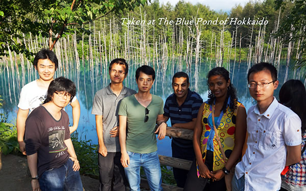
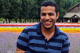
My colleagues representing to me as the source of every success and happiness I have lived in Japan. We are so interested in various events like doing barbecue party inside campus, eating Sushi and celebrating the end-year ceremony. From time to time, we organize trips to Hokkaido’s sightseeing like Tomita farm, Blue Pond and so on.
All in all, I sincerely discussed about my experience with spintronics in NSED, positively influencing on my future carrier, and so inviting all students to look for direction of electronics next few years.